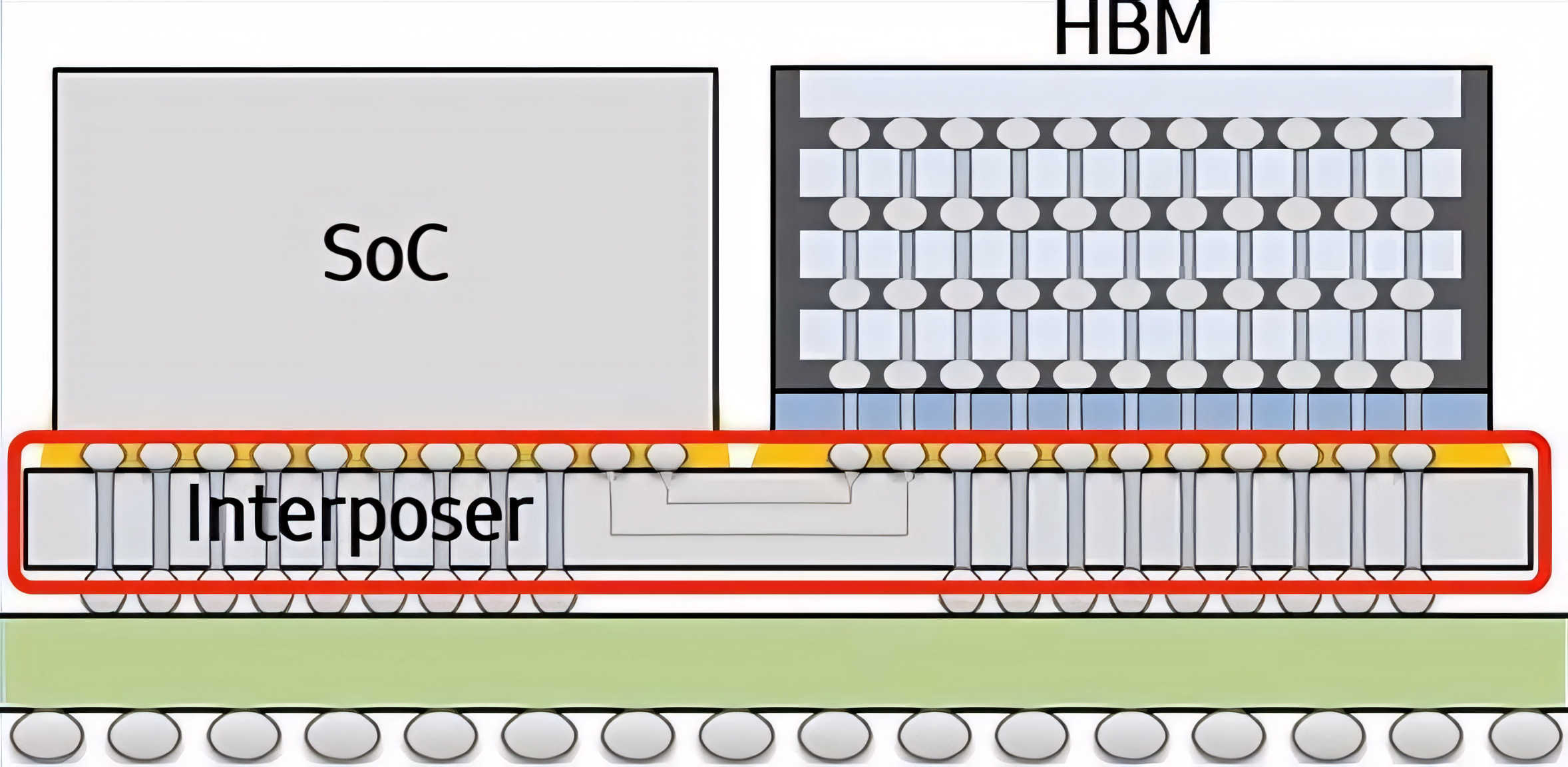
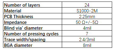
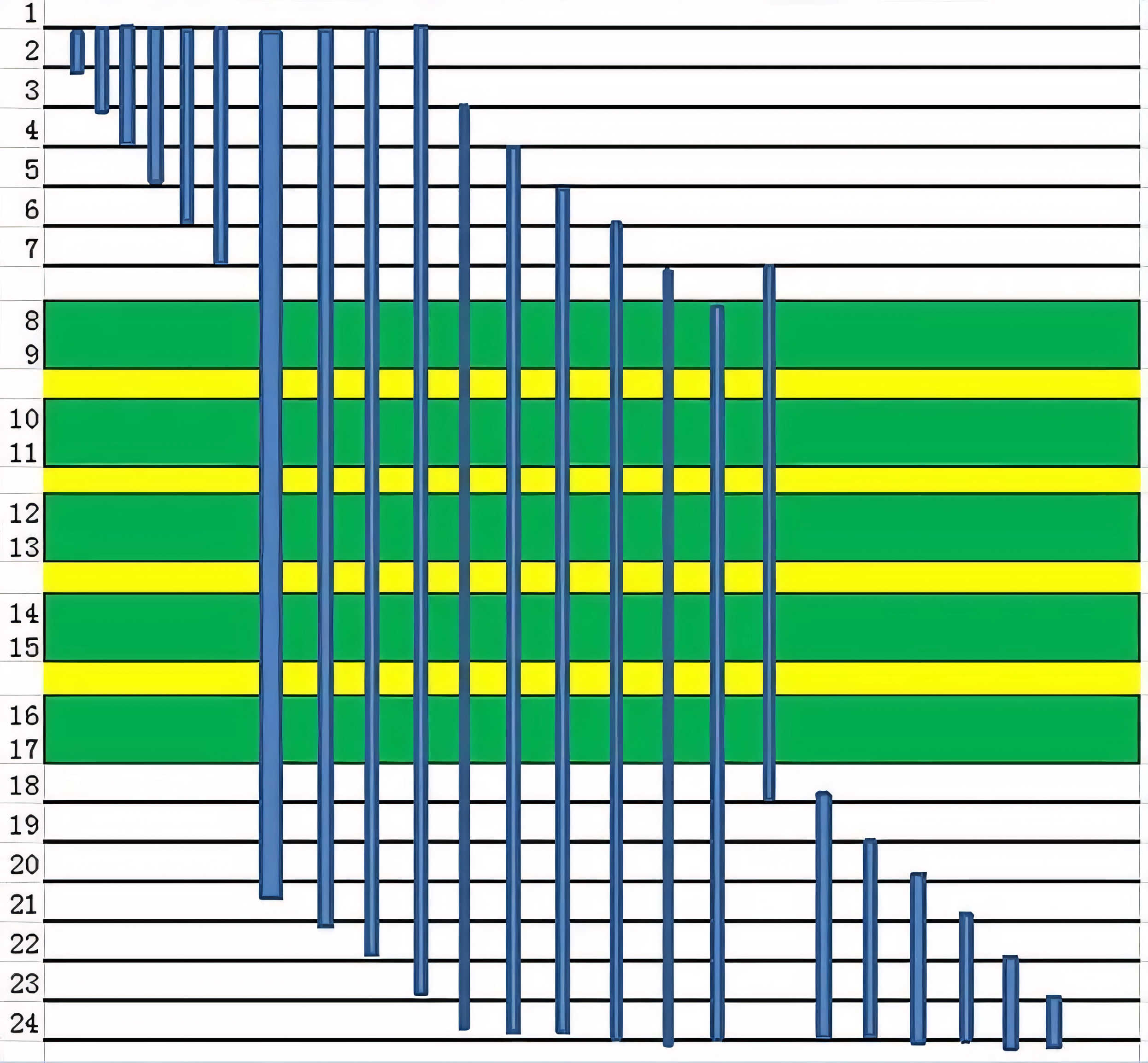
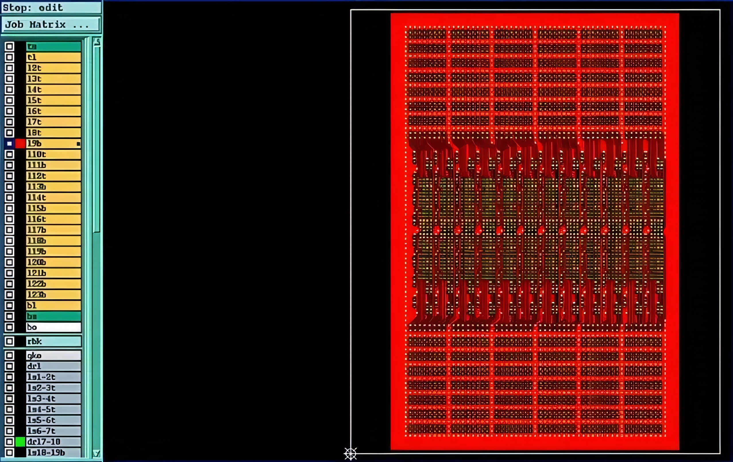
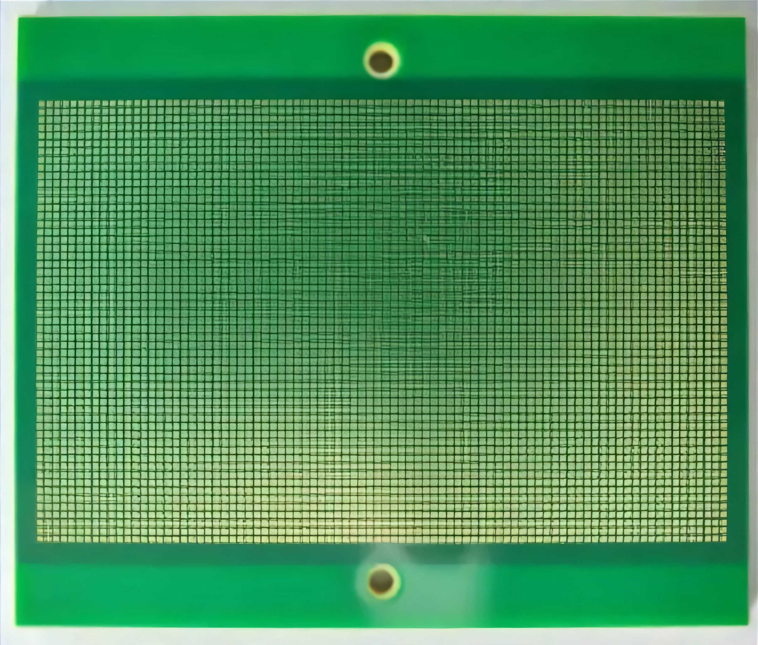
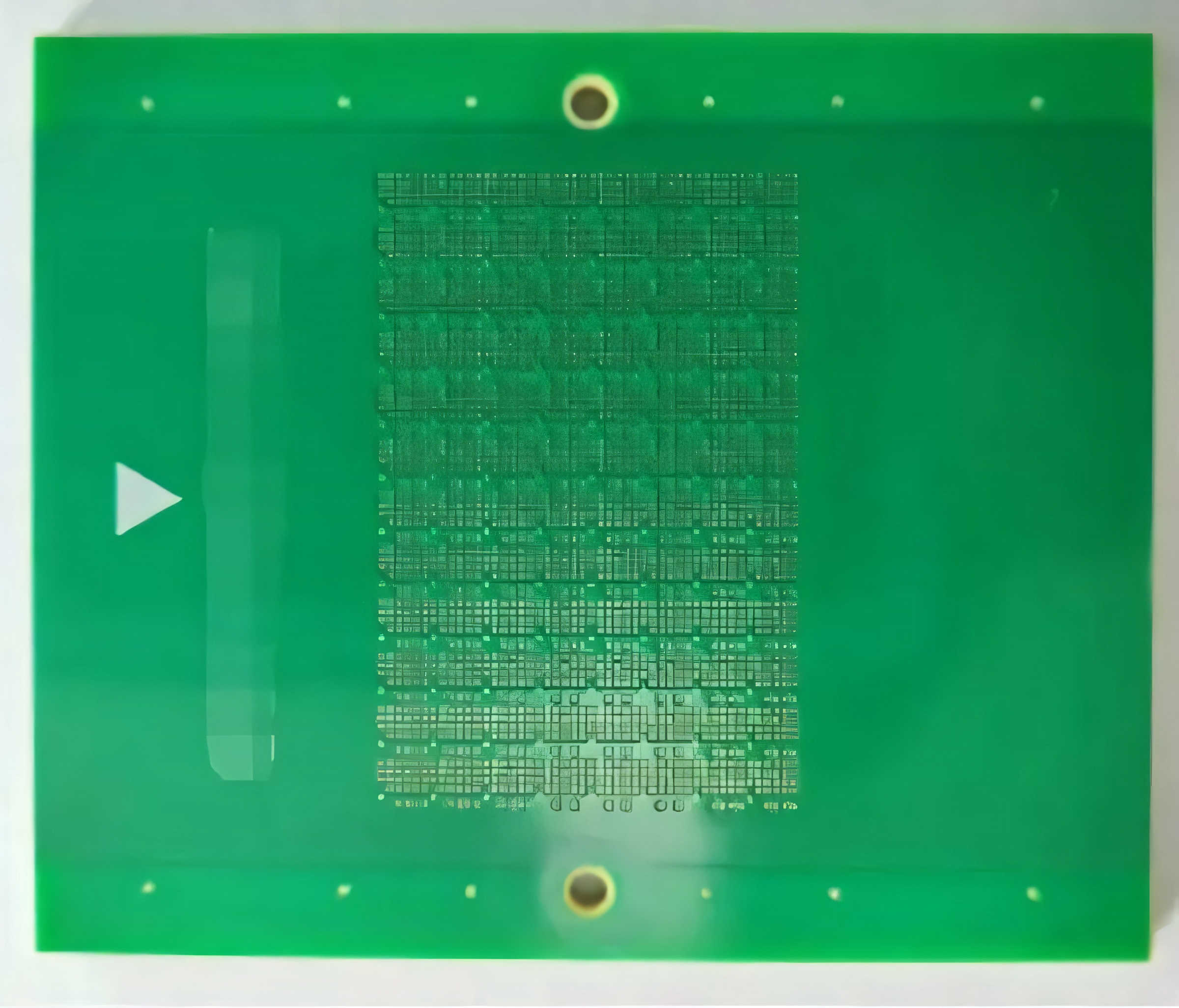
With the rapid progress in the integrated circuit industry, the complexity of chip connections has grown exponentially. Conventional PCB technology struggles to meet the demands of higher frequency and speed applications, posing significant challenges for stable and reliable chip-to-chip connections. As chip power consumption increases, managing heat becomes crucial to ensure uninterrupted performance. Consequently, the interposer PCB—a novel type of printed circuit board—has emerged as a solution to these problems. An interposer PCB is essentially a high-precision, multi-layer HDI (High-Density Interconnect) PCB that plays a pivotal role in connecting and integrating various electronic components. Acting as an intermediary layer, it facilitates chip-to-chip communication through pad leads and micro-bumps (uBump), while also incorporating routing within the interposer layer. This layer uses through-silicon vias (TSV) to connect upper and lower layers. This PCB's design features inner layers connected to outer layers via laser microvias and dense routing. It boasts a multi-structural layout with BGA (Ball Grid Array) connections on the top and pad connections on the bottom. Interposer PCBs bring immense value and importance to the performance optimization of integrated circuits. For one, they offer superior connection speeds and reliability for semiconductor products. Made from high-performance materials, interposer PCBs enable short-distance, high-density connections between integrated circuits, drastically boosting chip data transfer rates. Additionally, interposer PCB technology addresses signal integrity and power consumption issues. By connecting signal pins directly to the interposer layer, the length of signal transmission paths is reduced, minimizing signal loss and enhancing signal integrity. Furthermore, the interposer layer contributes to thermal management by effectively dissipating heat, keeping chip temperatures under control. Finally, interposer PCB technology allows for the integration of heterogeneous integrated circuits. By placing different functional chips on the same interposer layer, it enables seamless communication between various chips, thus enhancing the overall performance and efficiency of semiconductor products. In summary, interposer PCBs find extensive application in high-performance computing, artificial intelligence, data centers, and telecommunications. In high-performance computing systems, interposer technology connects multiple processing chips, amplifying computational capabilities. In AI, it accelerates neural network training and inference by enabling efficient interconnections between different chips. In data centers and communications, interposer technology offers higher transmission rates and bandwidth, meeting the needs of big data processing and high-speed communication. As a leading provider of high-end HDI PCBs, PCBWay stays ahead of market trends. In response to client demands for high-order arbitrary interconnection (Anylayer) HDI boards, our product research team has tackled numerous technical challenges, successfully developing high-layer, high-order arbitrary interconnection interposer PCBs. Here, we will showcase the details of this high-precision circuit product using a 24-layer, 6-order Anylayer HDI PCB as an example. 1. Product Specifications 2. Product Structure 3. Technical Challenges Challenge 1: The buried via PCB thickness from L7 to L18 is 1.0 mm, with a mechanical through-hole diameter of 0.1 mm, resulting in a hole aspect ratio of 10:1, making mechanical drilling challenging. Challenge 2: The BGA pitch is 0.35 mm, and the distance from the hole to the conductor trace is 0.13 mm, making it prone to misalignment during multiple laminations. Challenge 3: The trace width/spacing is 2.4/3 mil, featuring dense routing. Below are some routing diagrams. 4. Finished Product Images CNC turning is a subtractive manufacturing process in which pieces of material are rotated as a machine tool is fed to the piece, removing material to create a finished piece. It is primarily used to manufacture parts that are cylindrical in nature. We supply custom cnc turning service and CNC turning parts manufacturing Cnc Turning,Cnc Turning service,Cnc Turning Parts,Cnc Turning Services Ningbo Rongna Technology Co.,Ltd , https://www.service-machining.com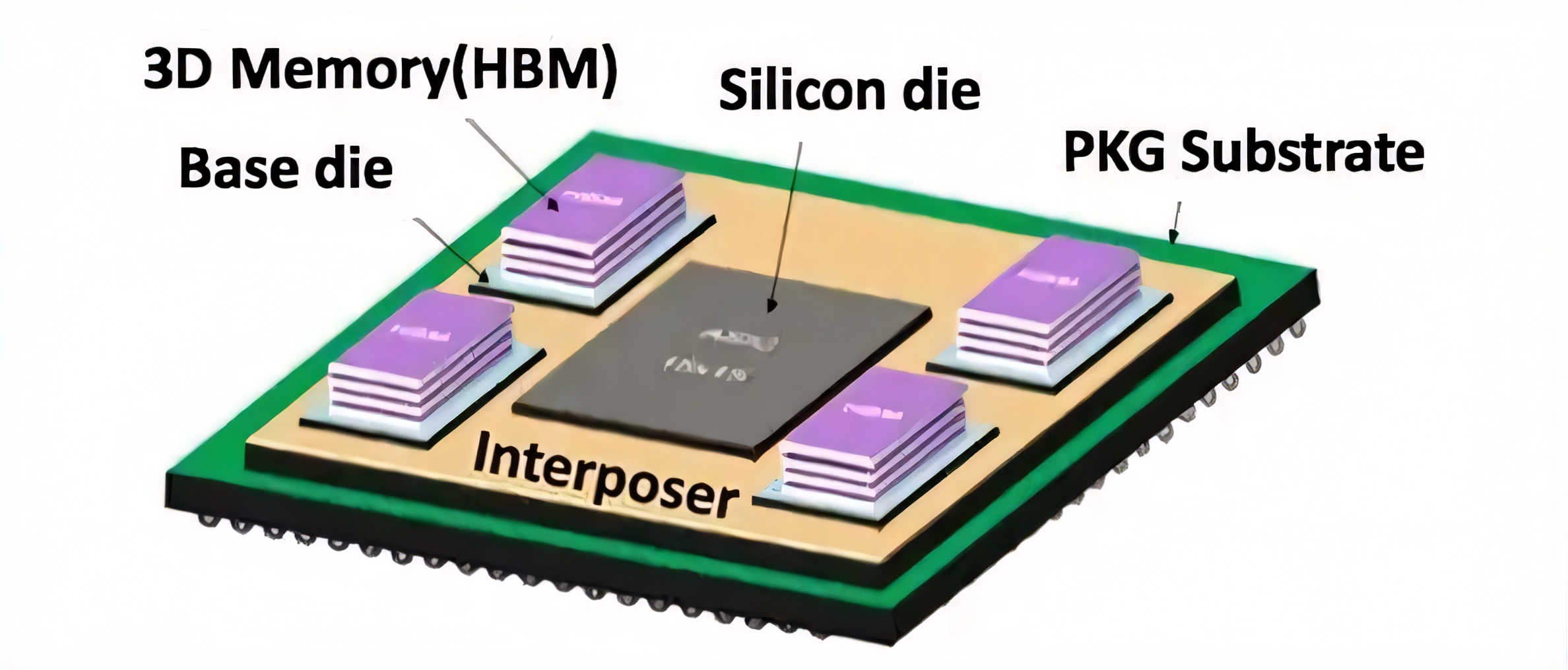
What is CNC TURNING?
Items processed by a lathe will be cylindrical and must be on-centre. Turned parts can range from simple rings to complex curved components. CNC turning is the most efficient way to mass-produce these kinds of parts.
Various cutting tools can be installed within the lathe tooling head to perform different cutting operations sequentially, to produce parts in a one-pass process. Straight cuts, tapers and contours can all be created by varying the angle and depth of the cut.
RongNa CNC Turning system is capable of cutting and holding different types of materials with complete accuracy and efficiency. CNC Turning to manufacture anything from furniture to garden tools to intricate machines and parts for cars and trucks etc.
We are professional CNC Turning Service company and custom CNC Turning Parts manufacturers in China, Our CNC Turning Center help with all kinds of projects and makes cuts of any work piece by changing the angle, the material and the type of cutting tool being used.